Sputtering: What It Is, How It Works, and PVD Applications
What is “sputtering”?
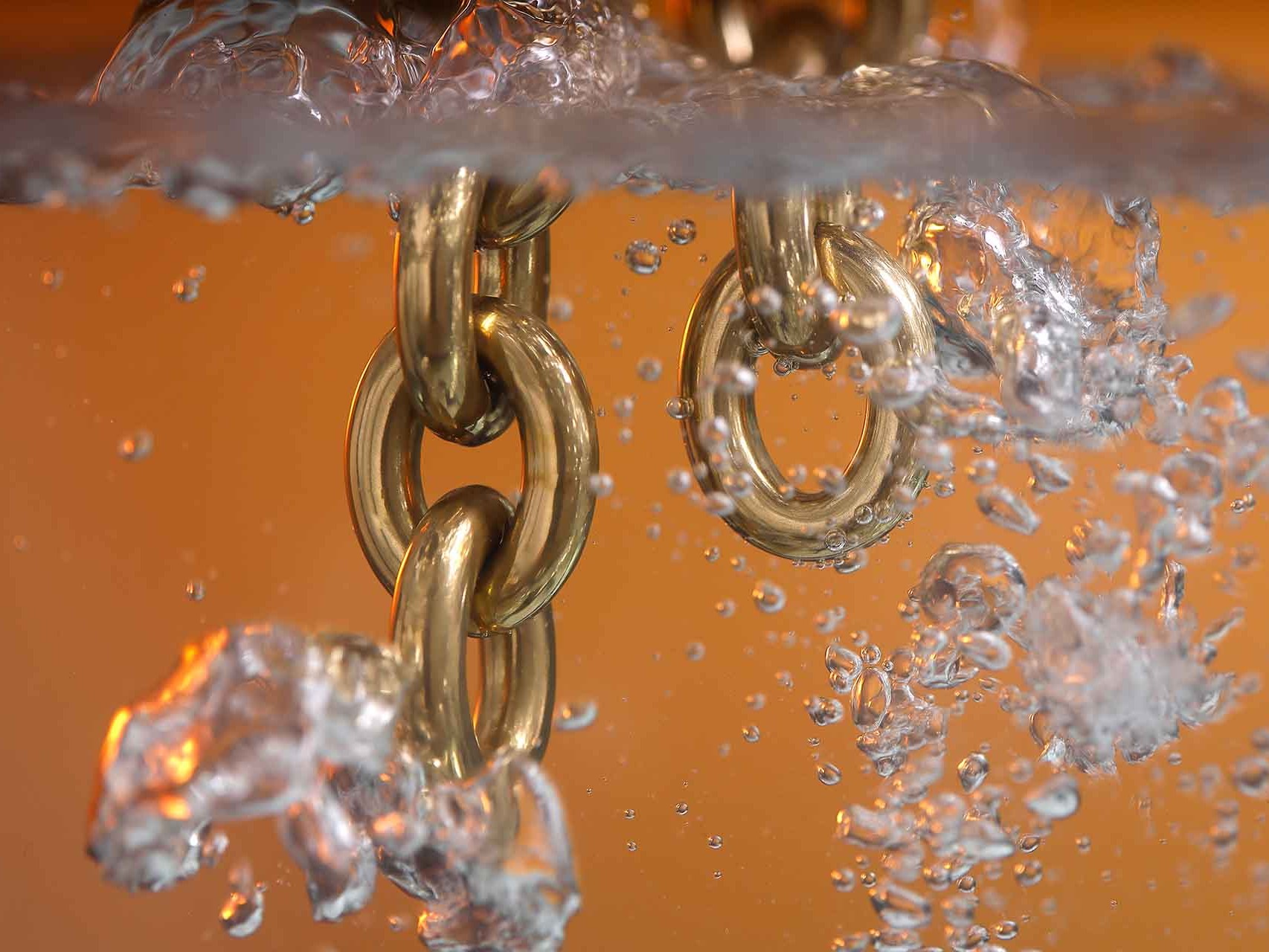
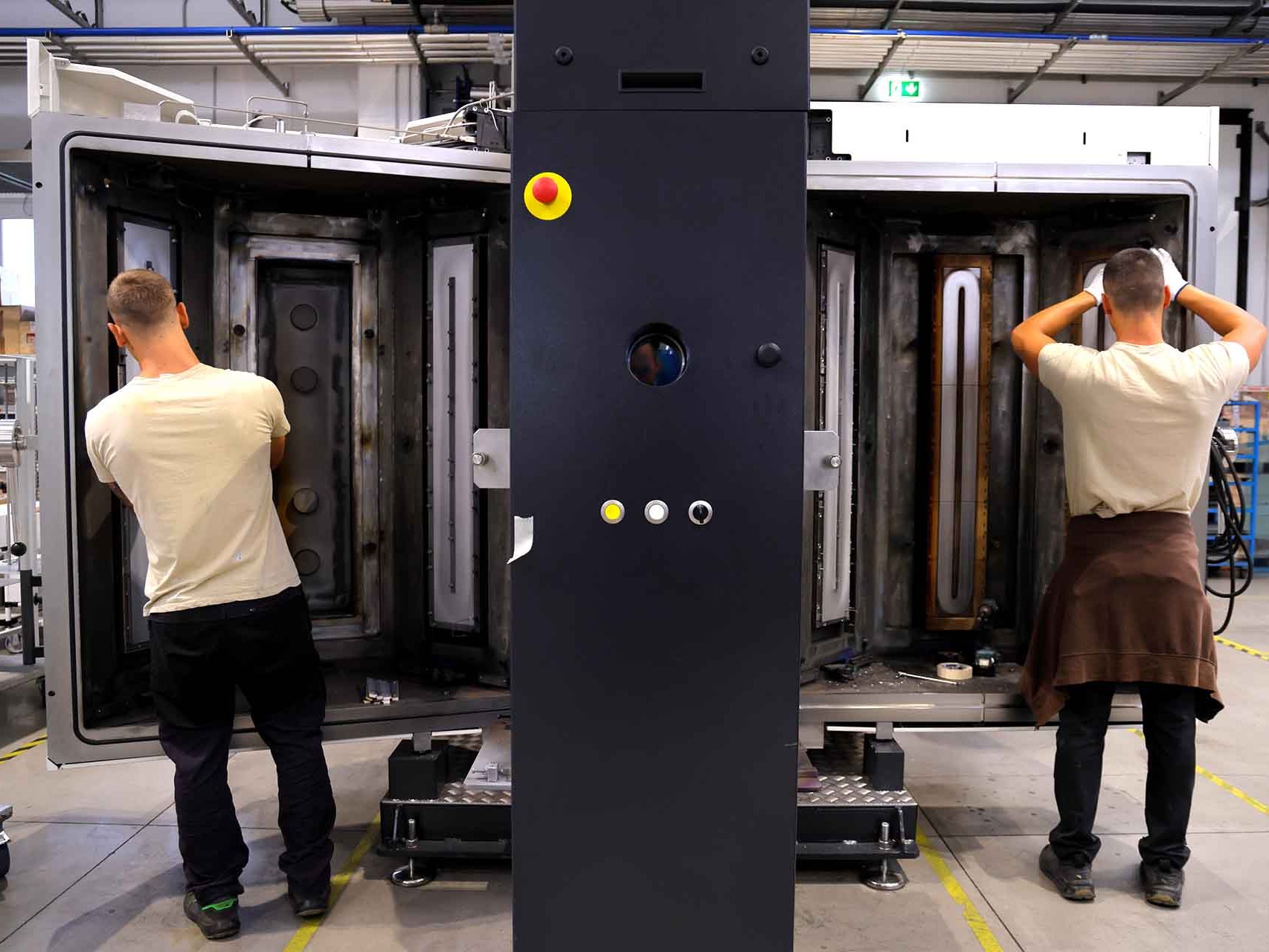
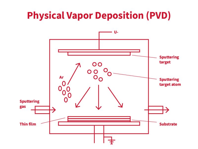
Sputtering is a Physical Vapor Deposition (PVD) technique used to create thin films on a substrate through the ion bombardment of a solid material, known as the target. The process is based on the controlled ejection of atoms from the target which, once released, deposit onto the surface to be coated, forming a compact and adherent layer.
Physical Principle: Plasma and Ion Bombardment
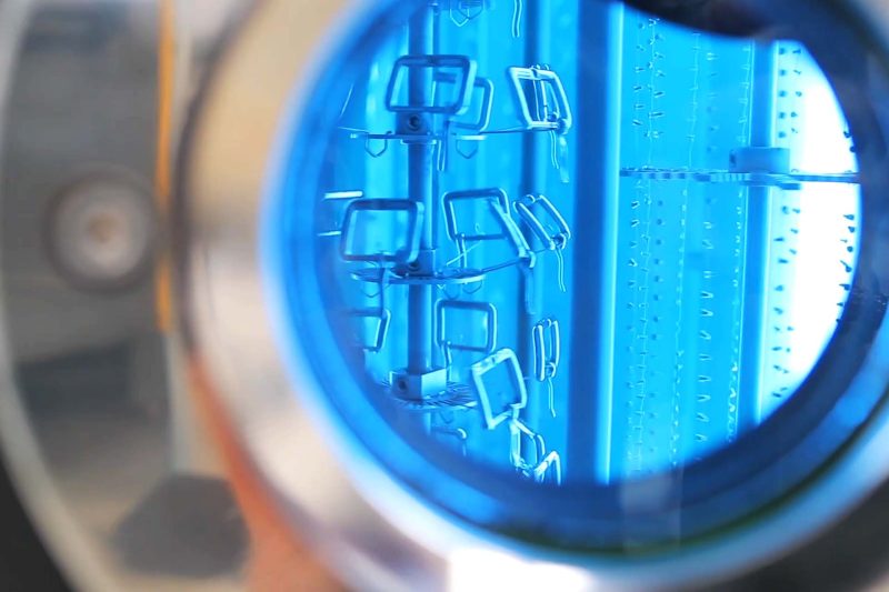
Sputtering takes place inside a vacuum chamber into which an inert gas, usually argon, is introduced. By applying a negative electrical potential to the targets, a plasma is generated, an ionized gas composed of electrons and positive ions.
The positive argon ions, accelerated by the electric field, strike the target with sufficient energy to eject atoms from its surface. This phenomenon, called ion bombardment, is purely physical (not chemical). The ejected atoms travel through the chamber and condense on the substrate, forming a thin film with high density and good adhesion.
Main Process Phases
- Creation of a vacuum in the deposition chamber.
- Introduction of the process gas (argon or a mixture with reactive gases).
- Ignition of the plasma through the application of an electrical potential.
- Ejection of atoms from the target and controlled growth of the film on the substrate.
- Thickness regulation, which is achieved by controlling the deposition time and energy parameters.
The coating thickness is adjusted by controlling the deposition time and energy parameters.
Operating Parameters and Their Impact
The performance of the film depends directly on the process parameters:
- Operating pressure: Affects the trajectory of the atoms and the uniformity of the coating. Lower pressures favor denser and more compact films.
- Applied power: Determines the energy of the ions and thus the deposition rate. Higher power increases the film’s growth rate.
- Gas type: Argon is used for non-reactive sputtering; the addition of oxygen or nitrogen allows for the deposition of oxides or nitrides (reactive sputtering).
- Target-to-substrate distance: Impacts thickness uniformity and distribution.
The precise control of these parameters allows for the modulation of the film’s microstructure, density, adhesion, and functional properties.
Types of Sputtering
- DC sputtering: Suitable for conductive materials.
- RF sputtering: Used for insulating materials.
- Magnetron sputtering: Integrates magnetic fields to increase plasma efficiency and improve the deposition rate.
Technical Advantages
- High adhesion to the substrate
- Dense and uniform films
- Excellent thickness control
- Deposition over large surfaces
- Ability to coat heat-sensitive materials
Among the main limitations are complex PVD equipment, high initial costs, and a generally lower deposition rate compared to other PVD techniques.
Application Sectors
Sputtering is widely used in various industrial sectors that employ PVD:
- Microelectronics: For the production of integrated circuits and thin conductive layers.
- Precision optics: For anti-reflective coatings, mirrors, and optical filters.
- Automotive: For functional and decorative treatments.
- Biomedical: For protective and biocompatible coatings.
Thanks to the high level of process control and the quality of the resulting films, sputtering represents a key technology in the creation of high-performance technical coatings.

Did you find the article interesting? Share it now.
Did you find something interesting? Contact us now!
LEM technicians are ready to address any questions or concerns you may have.
Request more information and discover our tailor-made solutions.